MOSFET: The Perfect Switch
I started going deeper into how chip-economics work when I realised I should probably get to know its history better. My first easy-read was Chip War to understand politics around chip production. While I have just completed a few chapters of it, it took me a few weeks to get through it. It took time since I went deep into every invention the book mentions, and what motivated it.
I am writing this blog to document my journey, and explain to others how the first transistors were made.
Edison’s Lightbulb
It all started with a lightbulb. A bulb works on the simple idea that when you heat up anything to really high temperature, it produces light. A modern bulb uses tungsten filament (insanely high melting point) which is a thin, coiled around piece of wire to get higher resistance. By doing this, you see light. An important factor of the lightbulb is that the glass-tube it is in has to be a vacuum (nowdays inert gas). This is because if there are even trace amount of Oxygen in the tube, the filament will oxidise rapidly at high temps and burn out.

Nothing new till now, everyone knows how lightbulb works. One day, Edison (or someone else, knowing Edison), noticed that after some time, the glass darkened everywhere except one sharp, clean stripe cast by the positive leg of the filament. That meant something electrically charged was flying off the negative side and getting blocked by the positive leg on its way to the glass.
Edison poked at this. He sealed a small metal plate inside the bulb, near the filament, and found that a current flowed across the empty vacuum to the plate, but only when the plate was connected to the positive side. Flip it, and nothing. Electricity was jumping through empty space, and only in one direction.
Fleming Valve
Edison patented his strange one-way current and promptly moved on. The effect sat on the shelf for about twenty years. Then, in 1904, John Ambrose Fleming dusted it off and turned it into the first true electronic device: the thermionic diode, better known as the Fleming valve.
The purpose of a diode is simple: act as a one-way valve for current. The construction is basically Edison’s experimental bulb: a filament, a metal plate near it, all sealed in a vacuum. The filament is heated until it glows, boiling off a cloud of electrons (thermionic emission again).
Now the trick:
- If the plate is positive relative to the filament, it pulls that electron cloud across the vacuum gap. Current flows.
- If the plate is negative, it pushes the electrons back. Since the plate is cold, there is no electron cloud around it so nothing to send the other way. No current flows.
Only the hot side can emit. That single asymmetry is what makes it one-way.
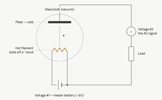
The cleanest demonstration of this is via the AC -> DC half-wave rectifier. Connect the bulb to the AC source, and a plate near the filament (at 0V). When the filament near the plate (near-side) is -vely charged, and far from the plate (far-side) is positively charged, current flows. It happens because there is an electron cloud which forms, which goes to both the far side and the plate, since there is a PD in both cases. On the other hand when near side is positive, there is no electron cloud at the plate (where the PD exists), hence no current.
The big loop is where the action is. It runs from the filament, across the vacuum gap, to the plate, then out through the AC source and the load, and back to the filament. Notice the AC source isn’t connected along the filament. It sits between the plate and the filament. So it doesn’t tilt the filament’s internal gradient at all. Instead, it lifts and drops the entire filament relative to the plate, by swings far bigger than that few-volt gradient. The filament’s two ends always differ by their few volts, but the AC throws both of them together far above or far below the plate.
That’s all a rectifier needs. During the half-cycle when the plate sits above the filament, the plate pulls the electron cloud across the gap and current flows around the big loop, through the load. During the other half-cycle, the plate sits below the filament and shoves the cloud back, and since the plate is cold, it has no cloud of its own to send the other way. The big loop is simply broken for that half-cycle. Feed in AC, and only one half of every wave makes it through: one-directional current. Half the wave survives, hence, half-wave rectifier.
This mental image is useful into how the diode’s circuit diagram symbol was created as well (a triangle pointing into a line). The line represents the filament, and the triangle represents the plate. Electrons move from the filament to the relatively positively charged plate. (Current moves in the opposite direction from the electron flow). Hence, the current can only flow in the direction of the triangle (from plate to the filament, because electrons flow in opposite direction).
By the way, its possible to create a Full-Wave Rectifier using multiple of these diodes as well. I will not go into details for it here
Lee De Forest’s Vacuum Tube
The next upgrade was pretty simple, instead of a diode, why not add a third electrode? It was of the shape of a sparse zigzag of wire, called a grid (later a mesh), sitting between the filament and the plate. Lee De Forest took Fleming’s valve and created a Triode.
The concept was that the grid acted as a sort of amplifier / gate. If the grid was at a slight negative voltage, the grid would repel the electron cloud from the filament, and lesser electrons could pass on through to the plate. Alternatively, if the grid was at a slight positive voltage, a lot more electrons would pass through the grid and on to the plate. If you can envision this, it was essentially a small PD inducing a much larger current in a different circuit! This was an amplifier.
And one more thing hides inside the amplifier. If a small grid voltage can smoothly throttle the current, then a slightly bigger one can slam it shut entirely: drive the grid negative enough and no current flows; relax it and the current floods through. The triode wasn’t just an amplifier, it was an electrically controlled switch.
People later optimised the triode too. The best configuration of the triode was a cylinder. A cyliderical mesh encircled the mesh, which itself was covered by a cylinderical plate. This configuration allowed for a much larger current amplification factor than a planar mesh.
It seems pretty important even at this point of the story, but to give more context one must understand what it was actually replacing. Before Vacuum Tube (Triode), there existed Electromechanical Relay. The relay is old, older than a lightbulb, and credited to Joseph Henry in 1835. It solved the same problem of amplification via simple electromagnetism. It gave the input current a simple job, flow through a coil of copper wire wrapped around some iron core, turning it into a magnet. The magnet then pulls down a small iron lever, and the tip of the lever, when pulled, closes a compeltely seperate circuit with its own, fresh, full strength battery. Pretty simple, a small input current leads to a stronger current in a different circuit.
But the relay has an obvious weakness: it’s a machine. A physical lever has to swing through the air, which takes milliseconds. The contacts spark, the moving parts wear out, and a room full of them clatters like a typewriter factory.
Which is what makes de Forest’s tube the real beginning of electronics. The triode does exactly the relay’s job: weak signal in, strong current controlled, but nothing inside it moves except electrons. It has no mechanical parts which are often prone to failure and wear out. Where the relay needs milliseconds to swing its arm, the grid’s electric field redirects the electron stream in nanoseconds
William Shockley’s Field Effect Transistor (FET)
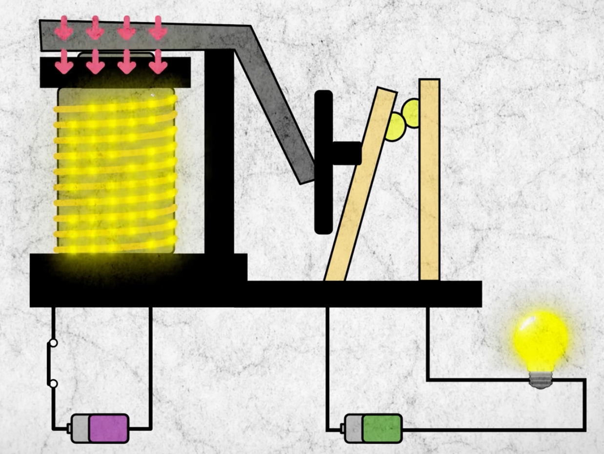
The jump from electromechanical relay to the vacuum tube was huge (almost a century huge). For about forty years, the vacuum tube ran the world. Radio, long-distance telephony, radar, and eventually the first electronic computers (ENIAC) were all powered by vacuum tubes. There were still multiple problems, since the vacuum tube was essentially powered by a light bulb. It was hot, the filament had to glow, by design, so every tube wasted watts just existing. It was fragile, glass bulbs, thin wires and like every lightbulb, it burned out. This required frequent replacement of vacuum tubes from the main circuitry.
A new solution was needed, one which did not depend on so many components. William Shockley was tasked with finding a solid-state solution, without so many mechanical components prone to failure. This is where the FET (Field Effect Transistor) was born. Semiconductors were all the hype even then, a family of misfit elements which were somewhere between an insulator and a conductor. Doping a semiconductor to make it behave like a conductor was also a known thing.
Shockley used a thin n-type doped semiconductor, and connected its two short sides to a battery. In this configuration, the semiconductor acts as a normal (but worse) conductor. Then, he introduced a metal plate which hovered slightly over the semiconductor’s long side, seperated by an insulator. When this side was connected with a PD, it created a Field Effect that either pulled or repelled electrons from the semiconductor. This was the Field Effect Transistor. The idea was that when connected across a positive PD, the electrons would be pulled towards the top (forming a thin line of electrons) where conduction would be stronger. And when it had negative PD, then the field would push the electrons away, starving this channel. If the slab was thin enough, a negative PD would stop any electron movement across the semiconductor.
I repeat, if a positive, much weaker PD across the plate, then the much stronger current would flow. If it was much weaker negative PD, then almost no current would flow. He had invented a solid state replacement of the vacuum tube.
Shockley then ran the experiment, it was supposed to work theoretically. But, when he made the connections and set the voltage, he observed “nothing measurable” across the semiconductor slab. He couldn’t explain it. Later, his colleagues explained it as a problem with “Surface States”. What happens is that Si in the semiconductor sits in a configuration of tetrahedron in the lattice. But, the topmost layer of this lattice are only connected to 3 Si atoms, not 4. This is the trap. When electrons are pulled upwards when the voltage is applied, the first few electrons gets trapped by these topmost layer of Si atoms. These immovable charges create a negative field of their own, which reduces the effect of the positive PD applied to the plate, and repels the electrons coming to the top layer. Hence, there is no electron channel created at the top layer, leading to no measurable difference in current conducted across the slab.
Bardeen and Brattain’s Point Contact Transistor
Through 1946 and 1947, Bardeen and Brattain weren’t trying to invent anything. They were debugging Shockley’s failure and in the middle of this detective work, in December 1947, that they assembled the Point Contact Transistor. They were not really able to resolve the main issue, but they figured out a way to sidestep it (not be bothered by the thin electron conducting layer which forms with FET).
In their design, they kept a n-doped Ge on top of a metal conductor layer called the base. This base was connected to the two loops, the input loop and output loop. The input loop was connected on the positive side with the Emitter, and the output loop was connected on the negative side with the Collector. The emitter and collector were two nodes which were supposed to be insanely close (approx 50 microns). Nothing existing there in the lab which could achieve this precision, so famously Brattain covered a plastic wedge with gold foil, and slit the peak of it with a razor to get our two nodes. These were then directly pressed on to the semiconductor slab.
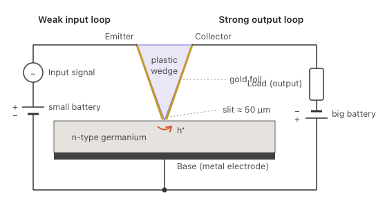
The circuit diagram should make clear what’s happening. Unlike the FET, there’s no external field reaching in to herd electrons. Instead, the weak input loop holds the emitter at a small positive voltage, and that positive contact pulls electrons out of the germanium beneath it. Every electron pulled out of a bond leaves behind a hole: so pulling electrons out is exactly the same event as injecting holes in. This is an important concept, and from here I’ll use this notion. A hole is nothing but the positive gap left where an electron should be; as neighboring electrons hop into the gap one by one, the gap itself glides the opposite way, behaving like a mobile positive charge (and moving in the same direction as conventional current). Holes are injected into the slab at the emitter. Each hole then has two options: get filled by one of the slab’s own free electrons (it’s n-type), or survive long enough to reach the collector. This leads to two core design choices:
- Collector must be insanley close to emitter: the hole has to reach it before some free electron occupies it. To maximise this probability, the collector must be very close to the emitter.
- Collector must be at high negative PD: the negative charge should attract the holes strongly, and the collector should also from strong reverse bias with the semiconductor.
These design choices lead to creation of a solid stage amplifier / switch. With no current in input loop, there is no current in output loop since there is a negative bias between collector and the slab (only some leakage current is there). The injected holes are the only key: each hole arriving at the collector lets current flow in a circuit that is otherwise shut off.
Shockley’s Junction Transistor
Shockley hated the PCT because it was not his. So, he took a few weeks alone where he worked furiously and came up with a better solution: The Junction Transistor. The main problem he solved was: PCT was a surface device, and surface held all the issues. Dangling bonds, electrodes pressed onto the surface etc etc. There were still too many components instead of a single susbtrate. He used the same “architecture” with emitter base and collector, just within the substrate itself. He created the “n-p-n” (or pnp for that matter) transistor. The slab will be a n-doped semiconductor, then a p-doped thin layer, then another n-doped layer. The first layer is the emitter, the second is the base, and the third is the collector.
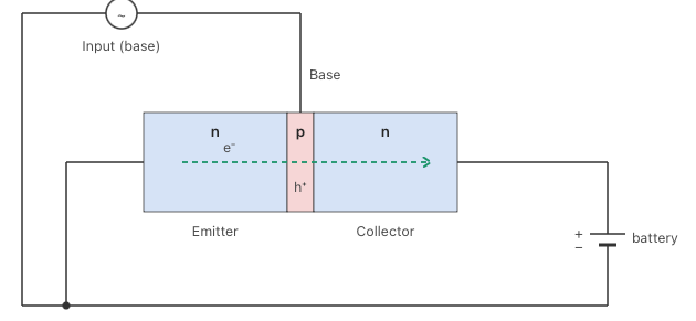
When left with no current, the n-p is forward bias, while the p-n is reverse bias, stopping the whole circuit from completing (except trace currents). Here, the emitter is connected to negative voltage, while the collecter is connected to positive (of the same battery). The base is connected to the input signal. Concept is simple, no matter the input signal, the electrons want to flow from emitter to the base. Now, since the base was so thin, they often did not completely combine with the holes in the base, and instead went on towards the collector. If the base was connected to a positive PD, supplying it constantly with holes, the electrons would from from emitter to base (and then towards the collector since the base is so thin). The collector was connected to a huge positive PD so it would keep attracting the electrons towards it. If the base was connected to 0 or negative PD, then the base would form a reverse bias with the collector, and the neg charged base would repel the electrons from the emitter.
This was an even better transistor than the PCT, since it involved none of the external elements of it. All of it was simply in the substrate itself.
Between the emitter and collector sit two junctions, back to back, facing opposite directions, so whichever way you apply the PD, one of them is always reverse-biased, and the device as a whole stays shut, leaking only a trace. The emitter is wired to the battery’s negative terminal and the collector to its big positive one, and still nothing flows: the electron crowd in the emitter combines with some holes in the base junction, but there is no flow from the base to the collector, so overtime it starts acquiring neg charge and repelling electrong flow. Now, add a positive PD to the base to supply holes and the emitter–base junction swings open: electrons flood from the emitter into the base. By rights they should all fall into the base’s holes and vanish, but the base is so thin that the vast majority sail straight across before being caught, and the collector’s huge positive pull sweeps them in. The small PD on base sustains a collector current a lot larger, set by how thin and lightly doped you make the base. If the PD across base is zero or negative, and the emitter–base junction is shut off, the flood stops, and the transistor stops working. We again have the amplifier / switch.
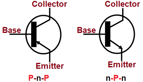
This can be simply seen in the circuit diagram, where for the n-p-n junction, current flows from base to emittor (meaning electrons go from the emittor to the base). The symbol is quite literally derived from the architecture of the transistor, which is pretty cool. In 1956, Shockley, Bardeen, and Brattain shared the Nobel Prize for their work on the transistor (Shockley had, by then, left Bell Labs and started his own company: Shockley Semiconductors in Paolo Alto)
MOSFET: The Perfect Switch
Shockley’s initial FET idea lost to the surface. The junction transistor won by retreating inside the crystal, away from the surface entirely. But the junction transistor, for all of its virtue, had one inelegence: its input isn’t free. The base must be continuously fed a current to keep the device on. Even though the electrons were flowing from the emitter to the collector. This is because even though its a thin layer, it will still combine with some electrons, in which case over time it will accummulate the negative charge. Unless constantly fed by a positive PD which absorbs these electrons, the transistor will eventually turn off. This required a small current, but multiply over a million transistors, it’s a tax on everything.
The dream device was still the original one. What everyone wanted was Shockley’s FET: a gate that controls by pure electric field, drawing no current at all, the way the triode’s grid floated above the stream. The only thing standing in the way was the surface and its dangling bonds.
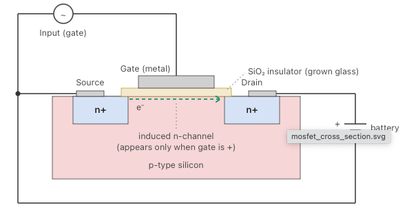
The fix, when it came, was pretty simple. Combine the dangling Si with something else. Mohamed Atalla noticed that if you heat a silicon wafer in oxygen or steam, the surface rusts: it grows a thin, glassy skin of silicon dioxide. But unlike iron rust or germanium rust, Silicon oxide was a marvel. It grows atom by atom out of the crystal itself, so the boundary between silicon and glass is nearly seamless. Atalla and his colleague Dawon Kahng built this device, and its name is just a list of its layers: Metal–Oxide–Semiconductor Field-Effect Transistor. MOSFET.
Take a p-type slab. Embed two pockets of heavily doped n-type into its surface, a short gap apart: these are the source and the drain (the FET family has its own terminal names; think of them as where electrons enter and leave). Across the gap between them, grow the oxide layer. On top of the oxide, deposit a metal plate: the gate. It is Shockley’s 1945 sketch, almost line for line — slab, insulator, plate — except now the insulator is grown from the crystal itself and the surface beneath it is clean.
With the gates at 0, the device is properly off. An electron trying to cross from source to drain faces n-type, then p-type, then n-type: two junctions back to back, one of them always locked. This was even higher this time since the p-type block was a huge slab. But once the gate is charged positive, then the electrons from the p-layer is pulled to the top, to form a thin continuous conductive sheet connecting the source to the drain. Current flows. Drop the gate to 0 (or negative), then the field evaporates and no current flows.
And here is why it’s the perfect switch. The gate sits on glass. No current flows into it: not a trickle, not a base current, nothing; it is controlled by field alone, through an insulator, exactly as Shockley drew it. Holding a MOSFET on or off costs essentially zero power; you only pay when switching. It has no filament to burn out, no contacts to wear, no lever to swing — and crucially, unlike everything before it, it gets better as it gets smaller: shrink the gap and it switches faster and cheaper. These propertie: free to hold, better when tiny, is the reason you can put billions of these on a chip and call it a processor. To better understand why it is free to hold, you need to understand one thing: two conductors with PD across them seperated by an insulator is a capacitor. A capacitor, once charged, mantains the charge and does not pull any further current. The plate and the p-layer became a capacitor, where there was no more need to pull in current from the input signal. This made it free of cost to mantian, and only cost needs to be paid was during transitions.
There’s a quiet irony in the materials, too. Germanium had been the workhorse of the transistor age: easier to purify, the metal of the point-contact and the first junction devices. But germanium’s oxide is useless: crumbly, even water-soluble. Silicon’s oxide is the best thin insulator nature offers. The MOSFET didn’t just pick silicon; it’s the reason the valley full of orchards became Silicon Valley and not Germanium Valley.
References and Notes
My main reference for the story was Chip War, chapter 1 -> 4 I also refered to Virtasium: How does a Transistor Work? and Why the First Computers Were Made Out of Lightbulbs to better understand and visualise stuff. Images are generated by Claude Fable 5 (except the replay transistor which is a screenshot from Vertisium video) Altough I put in maximal effort to write this on my own (I hate AI-slop), I did use Claude for fact-checking and storylining here and there.